ADC resolution is the level of one quantization step in the units of magnitude desired (such as volts to refer to the input, or counts to refer to the digital output levels). The resolution is the value of 1 lsb for a given ADC, as the step size that will be created from each lsb count just as the OP has computed: ~5 mV as 1 count in the OP's example, and that is correct for an ADC that provides 10 actual bits with a range of 0 to 5V.
ADC dynamic range is typically considered to be the ratio between a full scale sine wave and the noise floor of the device, specified as the total power over the unique digital frequency range (either $-f_s/2$ to $+f_s/2$ when we refer to two-sided spectrums, or DC to $+f_s/2$ when we refer to one-sided spectrums). This ratio is referred to as SINAD (Signal to Noise and Distortion Ratio). It is when dynamic range is defined this way specifically (ratio of power in a full scale sine to the total power in the noise of the ADC), then we get the relationship:
$$SINAD = 6.02 \text{ dB/bit} + 1.76 \text{ dB}$$
Definitions can vary so it is important to refer to the documentation for a specific ADC manufacturer when reading their datasheets. It is best to use the term SINAD directly as we can arrive at many other concepts of what dynamic range can mean, just as the OP has done- or other applications where we modify the dynamic range through subsequent filtering, or have different concepts in what a minimum discernable signal is, etc. Basically "dynamic range" on its own leaves a lot of room for different interpretations if there isn't a specific and clear definition with it. The OP is referring to Dynamic Range as the ratio of a full scale DC signal to one quantization level. This is a valid definition if clearly articulated, but that will not be a signal to noise ratio nor will it be equal to 6.02 dB/bit + 1.76 dB. In that case, just as the OP has determined, the ratio in dB would simply be 6.02 dB/bit.
Another term often associated with ADC dynamic range is ENOB (Effective number of bits). If the ADC was perfect, then the noise due to it's operation would be from quantization alone. Actual ADC's have additional noise sources (such as shot noise and spurious signals due to non-linearities) that increase the overall noise floor of the device, resulting in a reduced SINAD. The ENOB is a figure of merit that provides us the number of bits for a perfect ADC that would result in the same noise floor and it is derived from the dynamic range relating the power in a full scale sine wave to the total power in the noise (in contrast to the OP's dynamic range definition).
Thus, the relationship between SINAD and ENOB is given by rearranging the first equation given above as:
$$ENOB = \frac{SINAD-1.76}{6.02}$$
For the derivation of the above formula, and more details on the relationship between SINAD (SNR) and number of bits, and further introducing the effects of oversampling, please see DSP.SE post 40261.
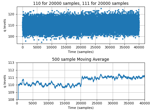
As an example of the possible confusion with dynamic range, below is a simulation with the OP's case of a 10 bit ADC with an input range of 0 to 5V, that has a dynamic range of 40 dB (for clarity, this example 10 bit ADC has a SINAD that is 40 dB). For this, I created showing what the output waveform could look like for this specific ADC if we were to input a DC level equivalent to 110 counts ($5 *110/2^{10}= .53711V$) for a duration of 20,000 samples, followed by a DC level of 111 counts ($5 * 111/2^{10} = .54199V$) counts for 20,000 samples. Note that the ADC output changes (in steps given by its resolution) over a range of roughly 100 to 120 counts. Importantly the lower plot shows what the result would be if we were to average multiple readings such that in this case, the ADC can discern the 1 count step! This shows that the ADC does still in fact "react" to the change of the input given we derived this result from the ADC output samples alone, and in fact we could use such averaging to discern even smaller fractions of a count. What we are seeing is that when we put in a higher value, all the samples that are output on average will be higher than when we put in a lower value. This is oversampling which can be used to increase the dynamic range of an ADC further, and thereby increasing ENOB.

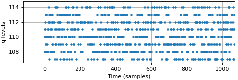
Below is a zoom in of the upper plot above, where we can discern the actual counts as the ADC output provides, representing the ADC resolution:

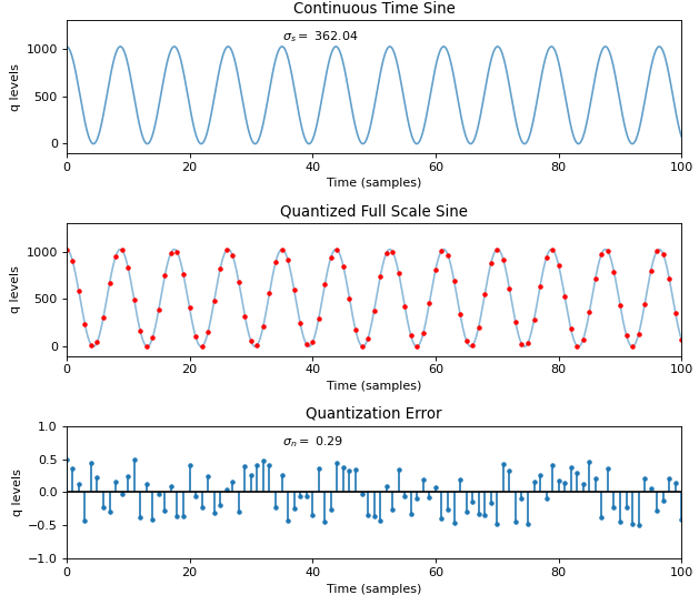
The 10 bit ADC, if it were perfect without the additional noise degradations (ENOB = 10 bits), under conditions of a full scale sine wave would result in the waveforms shown below, showing the analog input in units of counts, the quantized input, and as the difference between the two, the quantization error.

I computed in this experimental simulation for the ENOB =10 bits case, the standard deviation of the full-scale input sine wave as $\sigma_s = 362.04$ counts, and the standard deviation of the quantization noise as $\sigma_n = 0.29$ counts (note for the latter that the predicted quantization noise as detailed in the referenced post above is $1/\sqrt{12} = 0.2886$).
Thus the measured SINAD in dB is:
$$SINAD = 20log_{10}(\sigma_s/\sigma_n) \text{ dB}= 20log_{10}(362.04/0.29) \text{ dB}=61.90 \text{ dB}$$
And the predicted SINAD for a 10 bit converter is:
$$SINAD = 6.02 \text{ dB/bit} + 1.76 \text{ dB} = 61.96 \text{ dB}$$
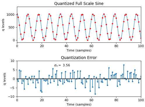
With the additional noise degradations, the sine wave as sampled above is still sampled into levels as given by 10 bits, but the additional noise is added to the sine wave effectively prior to being sampled, such that we still have the output changing in counts of the lsb, but with a much wider standard deviation as an error from the ideal sine wave with no noise added. So we still have 10 bits or 1024 unique levels coming out of the ADC, it's just that those levels include additional noise. This is shown in the graphic below where we see a much larger spread for quantization noise (as the error between what the output count tells us and the actual input signal):

Where here the standard deviation of the noise is now $\sigma_n = 3.56$ counts, and the measured SINAD is given as:
$$SINAD = 20log_{10}(\sigma_s/\sigma_n) \text{ dB}= 20log_{10}(362.04/3.56) \text{ dB}=40.15\text{ dB}$$
With this, we could back out the number of bits for an equivalent perfect ADC that would provide the same noise level as an rms quantity relative to a full scale sine wave:
$$ENOB = \frac{SINAD-1.76}{6.02} = \frac{40.15-1.76}{6.02}= 6.4 \text{ bits}$$
In summary the above shows the behavior of the LSB, and how it would toggle in all cases. But the representation of the resulting digital sample as either signal or noise (and ultimately a combination of the two) depends on the SINAD performance of the ADC.
The tutorial MT-003 by Walt Kester at Analog Devices is helpful in understanding all the noise sources that contribute to SINAD, including the variation in how this definition is used by different vendors.
The OP has continued questions in the comments:
"But we know that the ADC can't possibly measure signals below 4.88 mV if it has to have quantization levels of equally spaced in 1024 counts in the range from 0-5V. This is where my confusion lies"
This was for the case of a perfect 10 bit ADC with a range of 5V, such that one quantization level is $5/2^{10} = 4.88$ mV. And it is true that the ratio of full scale as 5V to 1 count as 4.88 mV or $1/2^{10}$ is $-20Log_{10}(2^{10}) = 60.2$ dB. Yet the formula "6.01 dB/bit + 1.76 dB" results in 61.86 dB and is associated with the "Effective Number of Bits" for 10 bits. So the OP is confused why we would call that the Effective Number of Bits, since a count level in dB that is 61.86 dB below a full scale DC signal of 5V would only be $5 \times 10^{-61.86/20}= 4.03$ mV.
This is because the dynamic range predicted by the formula 6.02 dB/bit + 1.76 is NOT the ratio of a full scale DC signal to a peak to peak count level ($q$). It is well defined as the ratio of the power in a full scale sinusoid (which to start is 3 dB lower than the power in the full scale DC signal!) to the ratio of the power in the quantization noise. The quantization noise is a uniform distribution $\pm q/2$, and for such a distribution the variance (which is the power) is $q/12$.
As far as not measuring signals below 4.88 mV- for a perfect ADC measuring a signal with no other added noise this is true, the ADC won't register any change just as the OP imagines if the signal never crosses a quantization threshold level. But if there are other noise sources present that exceed a threshold level, the ADC will be able to react to and measure much lower levels (as I demonstrated in the first graphic above). But that is really an aside, the main point is we are predicting a noise power level (as we would want for any SNR measurement), and that prediction applies under test with a full scale sine wave. The full scale sine wave will create a noise when sampled that has a standard deviation of $q/\sqrt{12}$. So if we measure actual noise levels higher than that, at the ADC output, then we can roll that into an equivalent perfect ADC with less bits, based on the standard deviation of the noise actually measured. What is convenient about this prediction, is that the power in the quantization noise as an absolute level, holds up quite well for other signals as long as the ADC doesn't go into clipping; so with that we can predict the SNR due to the ADC noise for other arbitrary waveforms. In the OP's case of a 6.4 bit ENOB and 5V peak signal, the standard deviation of the full scale sine wave is $V_p/\sqrt{2} = 1.77$ V rms. The standard deviation of the quantization noise is 40 dB lower or $1.77/10^{40/20} = 17.7$ mV rms. If we were to put in a lower level arbitrary waveform that had a standard deviation of 250 mV (for example), the standard deviation of the quantization noise would still be approximately 17.7 mV rms. This is the primary convenience of that formula for purpose of predicting SNR, and with that a measure of the dynamic range we can operate in based on our actual minimum SNR requirements.

