Can someone please provide an overview of sigma delta DAC? In particular, I would like to know how does the sigma delta modulator, which is digital, works for DAC. What is difference between sigma delta modulator for DAC and ADC?
2 Answers
I will show the comparison of a first order Sigma Delta DAC and first order Sigma Delta ADC and then use the ADC to further detail the operation for sigma delta modulation. I will also show how this is expanded to higher order structures.
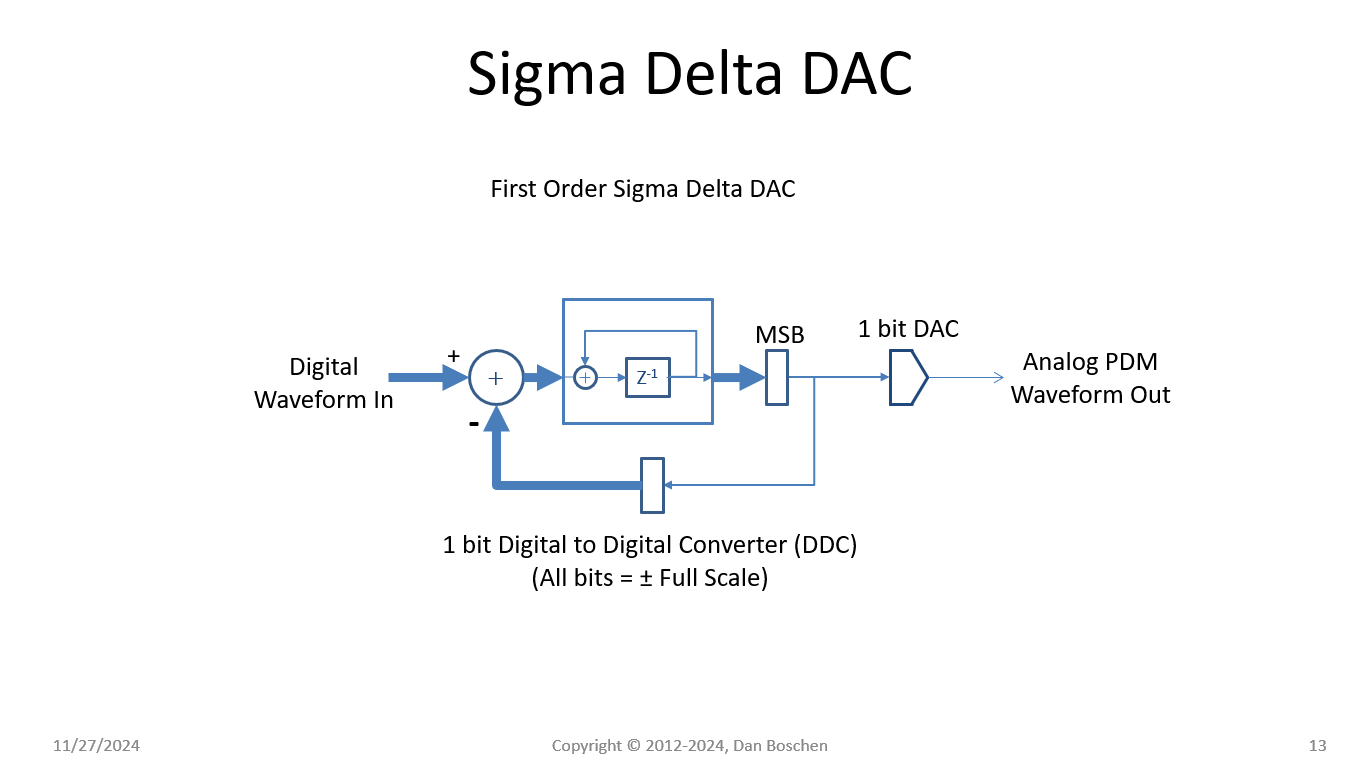
First I show the structure for a Sigma Delta DAC below with a simple explanation of its operation:
A higher precision digital waveform at the input, for purpose of explanation I will assume signed representation is subtracted from a full scale positive or negative result using the same number of bits. For example, if we had 8 bits coming in, this would have a range of -128 to +127 as signed representation given as integers. This would therefore be subtracted from either -128 or +127 depending on the state of the feedback.
The difference is applied to the input of an accumulator (the block with the $z^{-1}$ shown). So if the difference is a positive constant, the output of the accumulator would ramp up, and if the difference was a negative constant, the output of the accumulator would ramp down. The block shown as "MSB" selects the most significant bit of the word (the sign bit) and toggles the feedback state, and the output, whenever the accumulator causes the sign to change. The result, as we'll see in more detail below, creates a pulse density modulated output waveform- as a two level analog output. If we were to average the two-level output, the resulting average would converge to the precision given by the input. Averaging is a low-pass filtering process, and actual low pass filters designed for removing the higher frequency noise from the PDM waveform are more effective in producing the desired output in less time than a classical average would provide.
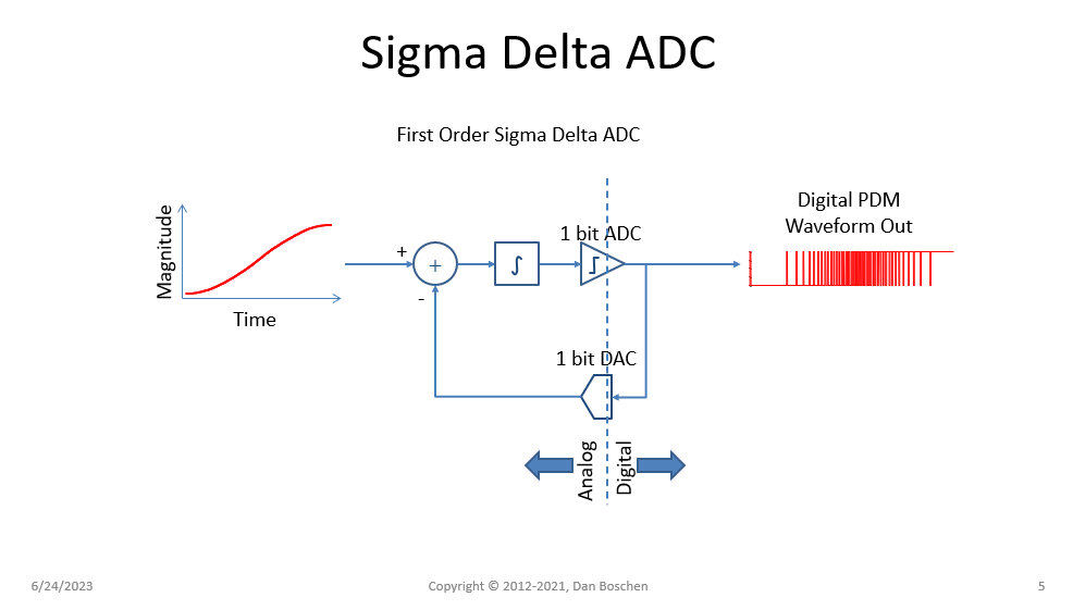
With that high level summary, for comparison the equivalent first order Sigma Delta ADC is shown below where we will see all the same functionality with digital and analog features swapped:
The operations are the same as described above for the DAC: The input is now an analog waveform (as shown here the first part of a sinusoid), the feedback is a two level analog waveform at the full scale range of the input, the difference is analog and provided to an integrator, which is an analog version of the digital accumulator. The integrator likewise will either ramp up or ramp down based on a constant difference value depending on if that difference is positive or negative. A 1 bit A/D Converter puts out a "1" or a "0" depending on if the output of the integrator is positive or negative. Importantly this selection occurs only at the update rate of the converter which as we will see results in the digital PDM waveform to be provided at the Sigma Delta ADC output.
So how does this work? I will show two sections of the sinusoidal input waveform shown above so that we see what happens when the input is low, and then close to mid scale, which should help provide further insight.
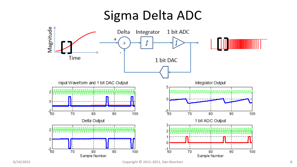
First when the input is low, I show below all the internal waveforms within the Sigma Delta ADC that results in a PDM waveform that would average to a low output value.
In this segment, the waveform starts low and slowing gets larger as the sinusoidal waveform proceeds in time. The feedback as I started it here is full scale low, so the difference is a small positive value, resulting in a slow rising ramp at the integrator output. The integrator as I started it was negative, so the output was low consistent with the full scale negative feedback (so all makes sense thus far, if we start in any other state it would proceed differently but with the same end result). Thus the output stays low for a relatively long time, since the accumulator is ramping up slowly. The point at which the output toggles is the next rising edge of our master clock (which is shown in green) AFTER the integrator has passed the zero crossing, which then causes the feedback to go positive. Due to the lower input value, the difference of the input and feedback will then snap to a large negative number (close to the largest it can be!), resulting in a relatively very fast slope downward at the accumulator output, back toward the zero crossing. For this reason, on the next rising edge of the sampling clock the integrator has already gone negative again causing the output to toggle back low--- thus we got very narrow high pulses with longer durations of low output. This is what we would expect for a low input level.
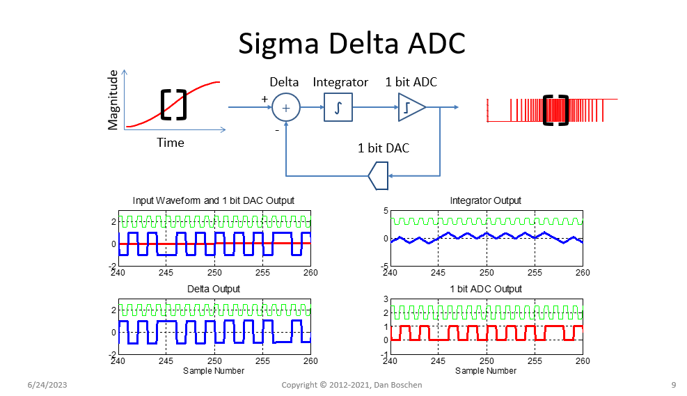
I show the same diagram for mid level values below, and the explanation for what is happening should now be obvious consistent with the above description, as to why in the mid level case we would get something close to a square wave out. We can also see now that for the high level case we would get narrow pulses going low with longer durations of high levels at the output:
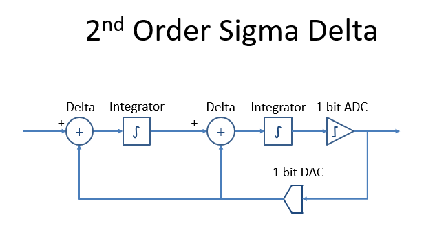
A first order architecture is useful for gaining a basic understanding of the fundamental operation but it is not recommended for general implementation. The implementation suffers from stronger "pattern noise" which manifests as high spurious interference in the spectrum of the generated waveform. Higher order sigma delta implementations both improve the achievable resolution and reduce the pattern noise artifacts. These are formed by adding additional integration (accumulation) stages in series, with a penalty in reducing the full range of the output while maintaining stability. Below shows a simple 2nd order Sigma Delta ADC as stages in series. To be aware of, the MASH architecture (multi-stage noise shaping), is a popular approach implemented with stable low order modulators, providing better stability when the full output range is needed, and also results in a multi-level output.
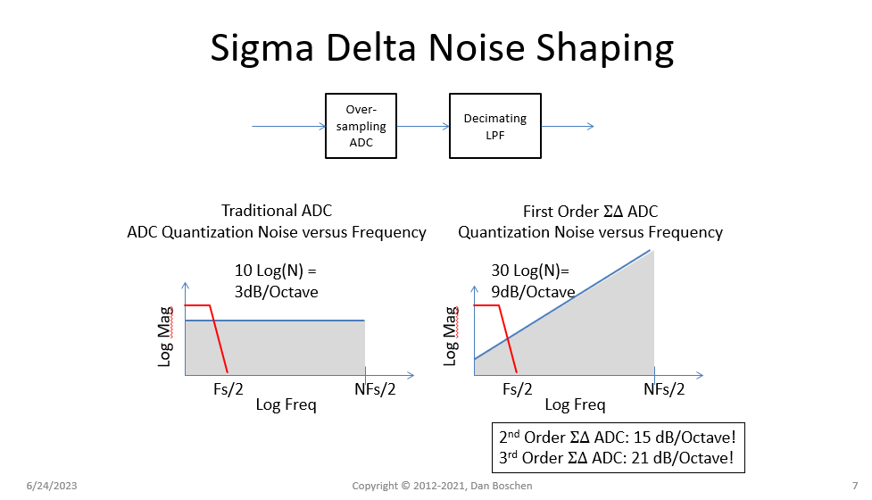
The feedback operation provides noise shaping resulting in the equivalent of very high precision for a relatively small amount of oversampling compared to traditional data converters. The benefit of noise shaping is introduced briefly with the graphic below:
How do I know this? I teach courses on DSP and Python related to wireless comm through dsprelated.com and the ieee (with new courses running soon!) and have implemented higher order sigma delta modulators for data converter and fractional frequency synthesizer applications. These graphics are out of my "DSP for Software Radio Course" which includes Sigma Delta modulation and much more details related to noise shaping.
-
$\begingroup$ Dan you need to more accurately model the effective gain of the comparator operation when you "linearize" the model and replace the comparator with an additive noise source. You can't just assume it's 1. What if you put a big non-inverting gain in front of the comparator? Would it change anything? Now what if you put that same gain in front of the additive noise source? Would that change anything? $\endgroup$ Commented Jun 26, 2023 at 17:28
-
$\begingroup$ @robertbristow-johnson completely understood if you are referring to trying to create a linear feedback model for such a non-linear system. That I get. $\endgroup$ Commented Jun 27, 2023 at 3:45
-
$\begingroup$ How else are you gonna model the noise shaping? $\endgroup$ Commented Jun 27, 2023 at 10:48
-
$\begingroup$ @robertbristow-johnson I am saying I agree with you. I've done approximate linearization for deriving the NTF with reasonable matching to the actual noise shape. $\endgroup$ Commented Jun 27, 2023 at 11:27
-
1$\begingroup$ The formula for the gain of the comparator is $$ \frac{\frac{\Delta}{2} \overline{|x|}}{\overline{x^2}} $$ where the comparator output is $\pm\frac{\Delta}{2}$ and $x$ is the input. $\endgroup$ Commented Jun 28, 2023 at 7:23
Disclaimer: I've only built one "true" sigma-delta DAC, and it was first-order because I was running it on a 25MHz FPGA and I only needed telephone-quality audio out of it. So rather than spending my clients money to have fun, I stuck with the basics.
There doesn't need to be much difference between the analog/digital sigma-delta modulator you might build for an ADC vs. the all-digital one you'd make for a DAC.
Both have a modulating element that takes a continuous (in the case of the ADC) or many-valued (in the case of the DAC) signal from a loop filter and, at each sample instant of the loop*, turns it into a 0 or a 1. Both translate that 0 or 1 to match the full scale of expected input values (with a carefully buffered digital output in the case of an ADC, and just a multiply or change of attitude in the case of the DAC). Both have a loop filter that conditions the output of the summing junction to perform the noise shaping that makes a sigma-delta modulator worthwhile.
Here's a chart that sums up the differences between the elements -- all of which are present in either type of sigma-delta device:
| function | ADC | DAC |
|---|---|---|
| modulating element | analog comparator | compare operation |
| modulator output | digital output | multiply operation |
| summing junction | analog circuit | subtraction operation |
| loop filter | analog filter | digital filter |
* Note that the sampling rate of that binary sampler needs to be significantly higher than the "normal" sample rate of the desired signal.
-
$\begingroup$ Don't you need to upsample your 48 kHz input to 64× (like 3 MHz) before the compare operation? Doesn't a ΣΔ DAC need the input to get upsampled to the high sample rate? $\endgroup$ Commented Jun 23, 2023 at 21:30
-
1$\begingroup$ Good point. I added that as a footnote -- but I was really trying to focus on the differences. Both ADC and DAC forms of the sigma-delta include massive oversampling so that the frequency-shaping has someplace to shape the noise into. (And the amount of oversampling depends on the complexity of the loop filter and following reconstruction filter -- 64x oversampling implies at at least a 3rd-order filtering for a 16-bit device, or it implies that the designer is deliberately allowing more noise in the high frequencies). $\endgroup$ Commented Jun 24, 2023 at 21:11

