Preamble: This answer is about timing recovery in a sense of symbol synchronization, i.e. finding the proper sampling phase of a baseband signal.
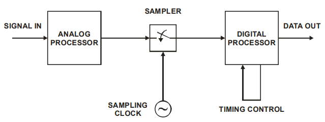
Based on the stated requirement of only 8 samples per symbol, I will assume that you are employing a fully digital approach to timing recovery. That means that you have no control over the times of sampling by ADC. The fully digital approach looks like this (this nice picture is from slides here):
From the right. The "digital processor" is your FPGA-based implementation of the timing recovery algorithm, including the selected Gardner algorithm to find a phase error. "Sampler" - is an ADC with fixed sampling rate, 8 samples per symbol. "Analog processor" - this is an analog front-end, which is implemented in your board outside of the FPGA. And "signal in" - is a baseband signal from your target communication channel.
In order to verify an implementation of your algorithm, you will want to model it, e.g. using a Matlab program or a Python script (whatever is more convenient). With the real signal samples from ADC you will be able to see the details of how your algorithm works in a long run, which otherwise is difficult to simulate in RTL and may be hard to debug when programmed on board. With a synthetic signal you can vary the parameters of the signal to see, how the algorithm reacts to it, and also you can plot a sigmoid for the TED, which can be very helpful.
About TED: Timing error detector (TED) is intended to detect a phase error in sampling. Based on the sign of its output, the timing recovery scheme will incrementally shift the sampling phase by a little step value, until the timing error becomes zero (or close to zero). This step value is usually selected to be 1-2% of a symbol period. Note, that with a fully digital timing recovery approach, when there is no actual control of the sampling phase, an interpolator is used instead, to fill the gaps between the signal samples. As a result the phase shift is made for the recreated version signal and not the real one.
Sampling phase error is defined by a phase difference between the transmitter, which generates symbols, and base sampling frequency of ADC (actual sampling frequency/8). Ideally the algorithm should be able to converge for arbitrary initial value of that error.
The answer to the question: In order to adequately model the initial phase error, the model must include not only a digital processor, but also a sampler. This means, that the input signal for the model should be continuous or oversampled. The degree of oversampling will define the resolution ability of your tests, i.e. how many different initial values you can provide. The goal can be 50-100 points per symbol period.
If you intended to use a real signal as an input of your model, you would use a logic analyzer to capture the signal at the input of the ADC with high enough frequency.
Alternatively, you may want to use a synthetic signal, that models a real one. Then you have to create its mathematical model. Usually you will start with random symbol values (as you did), then apply the modulation scheme (you will skip this if the symbol is a signal level), then apply a pulse shape (if the target transmitter does), then apply the distortions/pulse shaping relevant to your intended target communicating channel and analog front end (e.g. a low-pass filter can model the distortion of the signal in a twisted pair).
As you can see, the particular way of creating a synthetic signal will strongly depend on the type of the target communication channel.

