3
$\begingroup$

I was looking at the schematic for the small USRP B205-mini SDR from Ettus. I can't seem to find any switchable analog anti-aliasing filter on the input of the chip, or anything resembling a filter for that matter.

This would mean that the filtering is done inside the chip. But how? When using software like GNU Radio, you can basically choose an arbritary sample rate within the IC's specification. Does the chip have a huge filterbank for filtering the input that is switched in, depending on the sample rate, or how does it eliminate anti-aliasing?

$\endgroup$

1 Answer 1

2
$\begingroup$

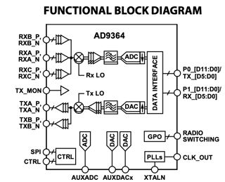
The key is the front end of the SDR. The first active component in the schematic is the AD9364 1 x 1 RF Agile Transceiver. This device is where the analog mixing and band limiting filtering, analog-to-digial conversion, and digital channelization occur.

enter image description here

Quoting from the data sheet:

The receiver includes 12-bit, Σ-Δ ADCs and adjustable sample rates that produce data streams from the received signals. The digitized signals can be conditioned further by a series of decimation filters and a fully programmable 128-tap FIR filter with additional decimation settings. The sample rate of each digital filter block is adjustable by changing decimation factors to produce the desired output data rate.

The initial band limiting occurs after the mixer. This provide anti-aliasing for the ADC. Any further decimation and associated anti-aliasing filtering occurs within the reconfigurable digital logic based on the selected decimation factors.

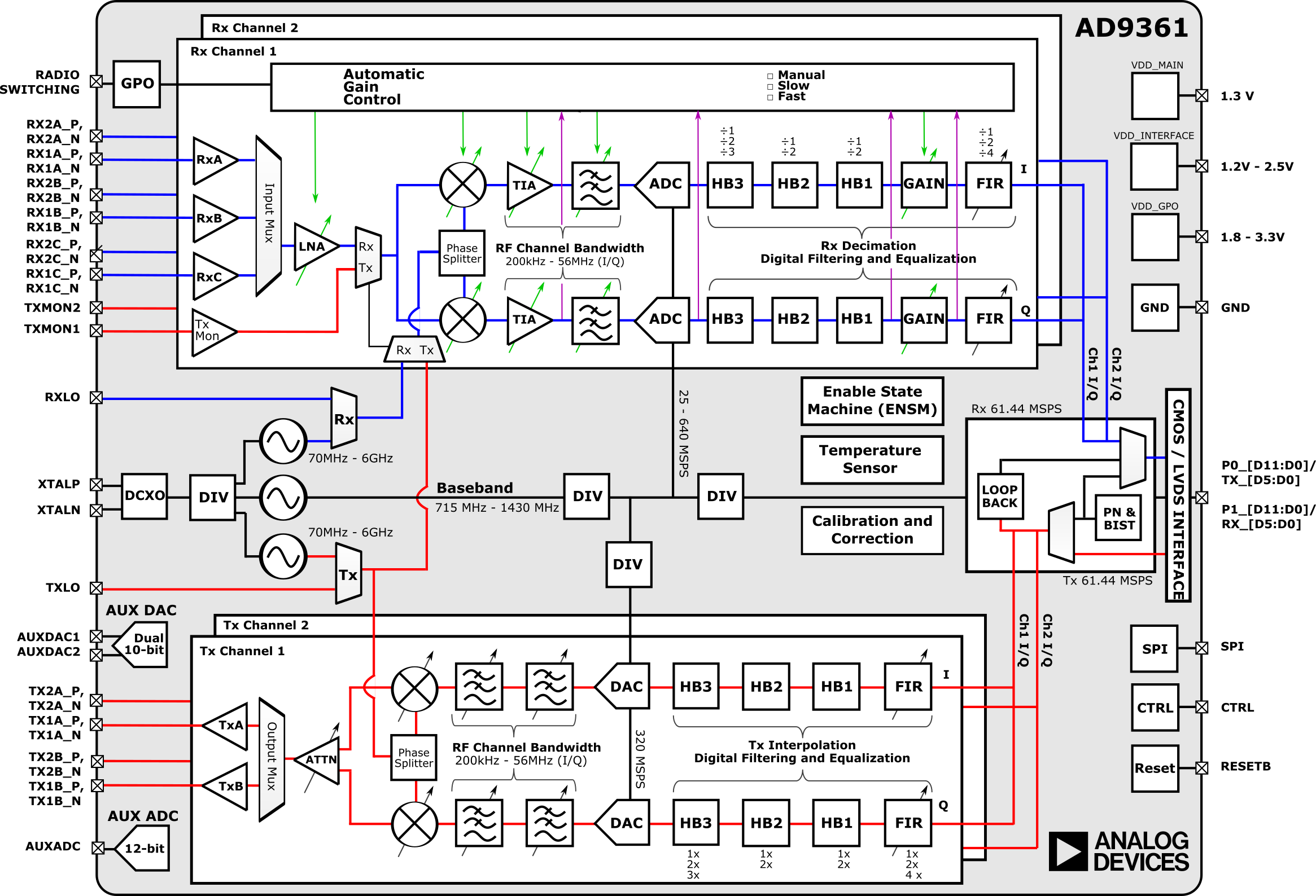
Here is a more detail diagram as suggested by user67081 (link to original).

enter image description here

A lot more detail can be found at the Analog Devices Wiki.

$\endgroup$
8
  • $\begingroup$ This is a more informative block diagram: wiki.analog.com/_media/resources/eval/user-guides/… Basically - the ad9361 has built in reconfigurable analog anti-aliasing filters prior to the ADC. The subsequent digital filters (FIRs + Halfbands) allow the ADC rate to be further decimated - note that there are a lot of constraints e.g. maximum ADC clock rate, PLL constraints, maximum rate through each of the digital filters, etc - but the gist of it is a combination of ADC clock rate + digital FIR configs enables a wide range of samplerates $\endgroup$
    – user67081
    Commented May 21, 2022 at 5:17
  • $\begingroup$ Thanks for your answer. So basically, the ADC in the RF tranceiver always runs at it highest sample rate(61.44 MSPS), and depending and how the user programs it, it decimate the signal to fit whatever samplerate the user wants on the digital side. Is this correct? And therefore it only needs to have a single anti-aliasing filter, to fit the 56MHz BW, after the mixer? $\endgroup$
    – Linkyyy
    Commented May 21, 2022 at 9:55
  • $\begingroup$ I thought the ADC data rate was actually changing, when you programmed different sample rates on the unit. $\endgroup$
    – Linkyyy
    Commented May 21, 2022 at 9:56
  • $\begingroup$ @user67081 thanks! I've added the more detailed digram to the answer. $\endgroup$ Commented May 21, 2022 at 10:05
  • $\begingroup$ @Linkyyy see the (Analog Devices Wiki)[wiki.analog.com/resources/eval/user-guides/ad-fmcomms2-ebz/…, there's a lot more detail about the functioning of this part there that is more digestible than the data sheet. $\endgroup$ Commented May 21, 2022 at 10:10

Your Answer

By clicking “Post Your Answer”, you agree to our terms of service and acknowledge you have read our privacy policy.

Not the answer you're looking for? Browse other questions tagged or ask your own question.