Update: The OP has stated in the comments below this post that the intention is to actually create output samples at a 15.36 KHz rate and that the sampling, as a simple submultiple of 200 MHz, can be done at a 125 KHz rate. This results in interpolate by $3 \times 2^7$ and decimating by $5^5$. With care of not letting the lowest rate go below 15.36 KHz, the following sequence could be implemented with a similar polyphase structure further detailed below for the 200 MHz to 245.76 KHz resampler:
125 KHz in, three successive stages of interpolate by 4, decimate by 5, followed by an interpolate by 6, decimate by 5, decimate by 5.
As a a polyphase the first bank would be 4 FIR filters each being loaded in parallel at the input rate of 125 KHz but the output computations would be done at the 4/5 rate of 100 KHz, the second stage would repeat this with 4 FIR filters each being loaded at the rate of 100KHz with the output computations done at the 4/5 rate of 80 KHz, the third stage identically would have it's outputs computed at 64 KHz. After these three interpolate by 5 and decimate by 4 polyphase stages, the following interpolate by 6 and decimate by 5 would be implemented as 6 polyphase filter each being loaded in parallel at the 64 KHz rate with outputs computed at the 6/5 rate of
76.8 KHz. The final decimate by 5 brings us to the desired output rate of 15.36 KHz. Having multiple smaller stages as I have done here, ultimately significantly reduces the computational requirements.
See the details below for the 200 MHz to 245.76KHz resampler that would follow a similar process.
—————-
Prior answer based on OP’s originally stated question:
If the OP only has a 200 MHz clock and wants to create output samples at the 245.76 KHz clock with samples produced at that actual clock rate with reference to the 200 MHz master clock, then a PLL would likely be needed to reclock/sample the data at the lower rate assuming such a clock rate is not already available (even if the data is sampled at 200 MHz and then interpolated as detailed below or with other approaches).
If the OP just wants to do rate matching between samples clocked in at 200 MHz to provide the same data at the 245.76 KHz rate, or just wants to produce the data that would be equivalent to that sampled at the lower rate, this can be accomplished with a fractional rate resampler on the data sampled at the 200 MHz clock rate or any reduced rate to the extent the existing analog anti-alias filter allows (otherwise modifications to that filter may also be required to avoid aliasing degradations). This is quite commonly done and particularly straightforward when your desired sample rate is a fractional ratio of the sampling clock. Further this will allow for any possible higher rate processing such as additional filtering on your data which may greatly simplify the analog anti-alias filter used.
This approach could proceed as follows:
Sample the data at 200 MSps.
Do any "high-rate" processing that would be helpful at this rate, in particular this would involve filtering prior to resampling the data (as part of the resampling architecture and necessary in the same regard that an anti-alias filter is required prior to any sampling).
The common factors of your two sample ratios of 200 MHz and 245.76 KHz are $5^7 /( 2^5 3)$. This means you can derive your desired lower sampling rate with the combination of interpolating by $2^5 3$ and decimating by $5^7$. As I will show, this can be accomplished efficiently and simply with polyphase filtering and will also neatly provide the samples at the output sampling rate desired.
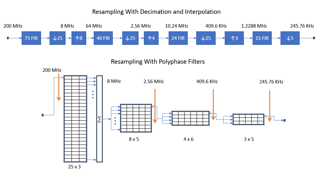
Below shows a candidate architecture showing a resampling as done with decimation and interpolation (filter to eliminate aliasing, downsample, upsample, interpolation filter, ...) and how this same process would map to polyphase filtering (using the same filter coefficients.
Notably, none of the internal clock rates shown need to be actually created, these are just the effective average rates. All nodes shown are internally buffered at any higher rate (likely the 200 MSps clock an sub-integer ratios. The only requirement is that each output sample is ready when clocked at the output clock rate and the buffering is sufficient to make up for the slop for the actual internal clocks used. As long as the input and output clock rates are synchronized, the overall architecture provides a consistent input/output rate so that no overflow / underflow can actually occur.
An output clock at 245.76 KHz is required in any event and if this is not phase-locked to the 200 MHz clock then additional care and consideration must be made on clock frequency offsets. Additional buffering would then be needed (and this is true for any implementation) to allow for the maximum number of sample differences based on the largest expected frequency offset and maximum time duration of the signal. This is only true when the ratio of the input sample rate to output sampling rate is actually higher than the numbers given (in which case buffers fill).
If it is known that there is no energy above 4 MHz after sampling with the ADC (due to current anti-alias filter used), then the first stage can be completely bypassed and decimation can be done by simply selecting every 25th sample at the ADC, OR dividing the ADC clock by 25 and sampling directly at 8 MSps. The 8 MSps data can then proceed with the architecture below at the 8 MHz node.

To follow the above diagram for the polyphase implementation, the first filter bank consists of 25 3-tap FIR filters with the first value of each filter input in sequence by the input data at the 200 MSps rate: each new sample fills the input of each subsequent filter, thus each filter has data shifting in at the lower 8 MHz rate and thus each filter in that bank operates as an 8 MSps FIR filter. Once each filter is input (after 25 input samples), the outputs of each of the 25 filters are summed to provide output samples at the 8 Msps rate and then the next 25 input samples are shifted in. Each output sample is entered into the next filter bank consisting of 8 5-tap FIR filters in parallel, such that the same output sample is input into all of the filters concurrently. The outputs of these 5 filters are commutated at the 64 MSps rate by sequencing through each output, but we only select every 25th value from this which provides the needed decimate by 25 as indicated in the upper diagram. Therefore the 2.56 MSps stream shown is achieved by selecting the first output, and then for the second sample effectively jumping forward 25 modulo 8 samples which ends up advancing to the next filter in the bank at this lower rate (notice that we never run anything at the 64 MSps rate, but immediately go the the 2.56 MSps rate!). The next interpolate by 4 and decimate by 25 is achieve is the 4x6 block as 25 modulo 4 at the 409.6 KSps output which also is an advance of one sample at that rate. Finally the 3x5 provides the interpolate by 3 which is then decimated by 5 as 5 modulo 3 or an advance of every other sample at this final output: We start with the top row as the first output sample, skip the second row and go to the bottom row as the second output sample, and then skip the top row and go to the second row as the third output sample, and so on (or simply reorder the rows to be 1-3-2). This results in a highly efficient implementation considering the relatively low clock rates in which all the filters have to operate. Note that the number of coefficients used in each of the filter banks comes directly from the originating resampling design as in the upper portion of the figure, and this is given by the passband and stopband requirements of these filters which is driven by overall distortion requirements. Actual numbers needed could be more or less than what I show here depending on the actual requirements. Please refer to this post for further details on the implementation of polyphase filter resampling. After reading the details there, the following example of the first decimate by 25 polyphase section will be more meaningful.
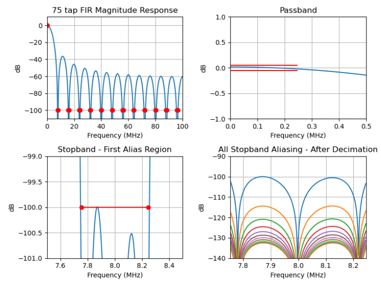
What follows demonstrates the performance that can be achieved in terms of minimizing distortion and optimizing resources by concentrating filter rejection only where it is needed using multiband least squares filter design (with firls in MATLAB, Octave and Python scipy.signal). Below is the frequency response of the 75 tap FIR that I mapped into the first 25x3 polyphase filter bank, where the stop-bands were defined by the locations of the red dots in the figure, minimizing the number of coefficients needed. Here I confirmed my initial 75 tap estimate was sufficient for a design requirement of less than 0.05 dB passband ripple and greater than 100 dB of rejection for any of the 12 decimation regions that could fold into the DC to 245.76 KHz desired passband. The coefficients of this same FIR filter map directly to the coefficients used in the polyphase filter bank with "row to column" mapping by decimating the same FIR filter coefficients resulting in all-pass filters of the same input with different fractional delays (polyphase). Note how with this approach we can quantify all distortion easily in the design process directly and modify the complexity accordingly (less coefficients if more distortion is acceptable).


